Low-dimensional Topological Matter
Our group is developing new thin film materials and epitaxial heterostructures based on recently discovered classes of topological materials, such as three-dimensional Dirac and Weyl semimetals. We synthesize topological thin films with high materials perfection and carrier mobilities using molecular beam epitaxy. One focus of our research is to gain a fundamental understanding of how nontrivial topological electronic states control the properties and phenomena in thin films and heterostructures and how we can use heterostructures to manipulate topological states. We use approaches such as strain, electrostatic confinement, and symmetry engineering, as well as fine-tuning by electric field effect. We seek to control and engineer these unique electronic states and to identify new opportunities for future electronic and quantum devices.
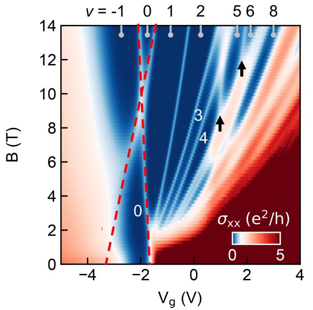
Quantum Transport
Quantum transport measurements are powerful techniques to characterize and discover new states of matter. For example, the image on the left shows the Landau level spectrum of a 20 nm thin film of cadmium arsenide that is in a two-dimensional topological insulator state as a result of quantum confinement.
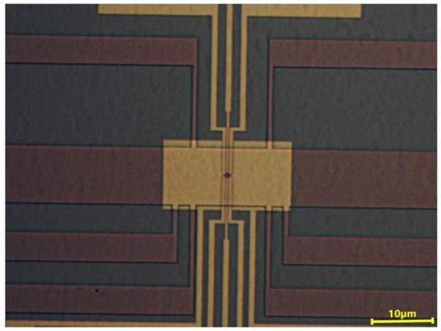
Quantum Devices
We are interested in building solid-state platforms that can host topological qubits and that can coherently control quantum phenomena. For example, the image on the left shows an electron interferometer fabricated by electron beam lithography in UCSB's nanofab.
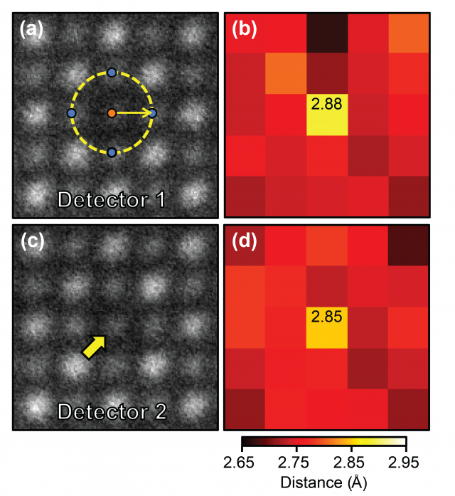
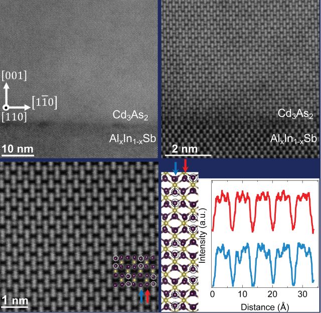
Quantitative Scanning Transmission Electron Microscopy
Our group has advanced in quantitative scanning transmission electron microscopy (STEM) techniques to a point that they now allow for detecting individual point defects, such as dopant atoms, and to quantify the atomic structure around these defects. For example, we have combined variable-angle, quantitative STEM and rigid registration methods to identify atomic columns containing vacancies in SrTiO3 and determined atom relaxations around them. These advances open up new insights into the mechanisms by which defects control materials properties. We are pursuing new directions in quantitative STEM using a newly acquired aberration corrected STEM in UCSB's microscopy facility (Spectra 200).